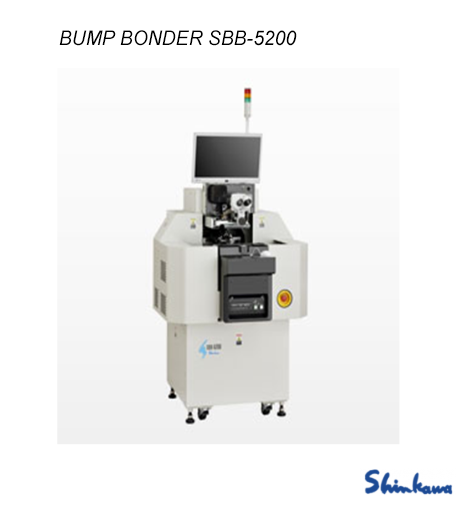
Specifications:
• High-speed bonding of 30 ms/bump based on Wire Bonder model UTC-5000
• Capable of handling up to 6-inch wafers by incorporating wafer rotary stage
※8-inch wafer handling capability (1 wafer stage) scheduled to be developed.
• Equipped with Two wafer stages with temperature up/down control function, reducing wafer changeover time and increasing productivity
• Capable of stable 45 μm pad pitch bonding with low vibration, high-speed drive using Shinkawa NRS technology
• Automatic correction of capillary tip position by Shinkawa RPS technology, enabling high accuracy bond placement and reducing work for capillary change
• Automatic free air ball monitor function (FAM) measuring free air ball size
• Multiple choices for surface contact detection at bonding, with "Force detection mode" to detect changes in force in real time as well as conventional "Positional detection mode," enabling stable bonding quality
• Bonding Accuracy: ±2.5 μm(3σ)Using Shinkawa standard device
• Correction of Bonding Position: System to check and correct capillary offset prior to bonding through Shinkawa RPS
• Bonding Speed: 30 ms/ bump (without reverse) Using Shinkawa standard device
• Bonding Wire Length: 8 mm maximum (Varies depending on device conditions)
• Resolution: XY-table: 0.1 μm Z-axis: 0.1 μm
• Vibration Control: Shinkawa NRS - Non Reaction Servo System
• Bonding Area: Maximum φ150 mm (6-inch wafer)
• Wire Size: Au φ15–32 μm
• Bonding Force: Maximum 4.9 N
• No. of Bonding Bumps: 30,000 bumps maximum
• Wafer Stage: 2 wafer stages for 6-inch wafers ※with temperature up/down control function
• Wafer Size: Size Maximum 6 inches
(Conversion parts are required when wafer size changes.)
• Thickness: 0.15–0.6 mm
(Conversion parts may be required when wafer thickness changes.)
• Production Management: Management of equipment availability through production management monitoring screen |